
Nano-Scale MoS2: Frontier Research in New Material Applications
2026-08-11
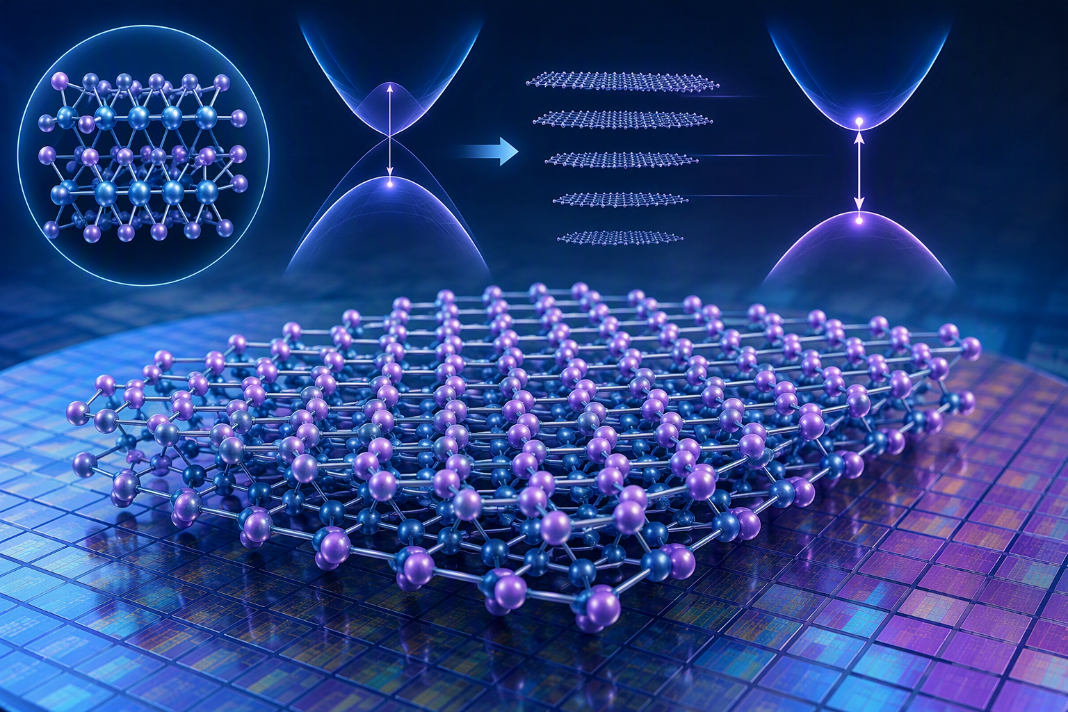
Nano-scale molybdenum disulfide, as a representative transition metal dichalcogenide, is evolving from a traditional lubricating material into a research focus in semiconductor, catalysis, and energy storage fields. When the thickness of MoS2 is reduced to the atomic layer level, its bandgap structure transitions from indirect to direct (approximately 1.8 eV), a quantum confinement effect that opens entirely new pathways for optoelectronic devices and flexible electronics. In December 2024, the National Standardization Administration of China released GB/T 44935-2024 "Nanotechnology - Measurement of the Number of Layers of Molybdenum Disulfide Flakes - Raman Spectroscopy Method," which officially took effect on July 1, 2025, marking the standardization of nano-scale MoS2 characterization.
Breakthroughs in Two-Dimensional Semiconductors
The progress of nano-scale MoS2 in the semiconductor field is particularly noteworthy. In October 2025, a Chinese research team reported the world's first 6-inch wafer-scale single crystal of two-dimensional transition metal chalcogenide semiconductor, with a single-domain alignment rate exceeding 99% on a 150 mm wafer. In July 2026, China's first 8-inch two-dimensional semiconductor process line completed full-line integration, with a process yield exceeding 99.99%, targeting equivalent 5 nm silicon-based chip production by 2029. TSMC also demonstrated 300 mm wafer-scale 50 nm contact gate pitch two-dimensional n/pFET integrated devices at the VLSI Symposium in June 2026, indicating that international giants are accelerating the transition of two-dimensional transistors from laboratory to production.
The core of these breakthroughs lies in the atomically ultra-thin channel properties of nano-scale MoS2. Compared with silicon-based materials, single-layer MoS2 has a thickness of only approximately 0.65 nm, enabling natural strong gate control at short channel scales and effectively suppressing short-channel effects and quantum tunneling leakage. This makes MoS2 one of the most promising non-silicon channel materials for the post-Moore era.
Catalysis and Energy Storage Applications
In the electrocatalysis field, nano-scale MoS2 is considered a strong candidate to replace platinum-based catalysts due to the high-density exposure of its edge active sites. Research shows that near-atomic-layer MoS2 nanosheets synthesized through functionalized graphene quantum dot induction can significantly enhance hydrogen evolution reaction (HER) catalytic activity. Porous MoS2 structures decorated with Pt nanoclusters prepared by CVD methods exhibit an overpotential as low as 43 mV and a Tafel slope of 56 mV/dec, approaching the activity level of commercial platinum-carbon catalysts.
In energy storage, a composite structure of MoS2 nanopetals and carbon quantum dots achieved an overall efficiency of 4.4% and a storage efficiency of 34% in photocapacitor devices. A semiconductor nanojunction constructed from MoS2 nanosheets and TiO2 achieved a Faradaic efficiency of 65.52% in photoelectrocatalytic nitrogen reduction to ammonia, providing a new approach for nitrogen fixation under ambient conditions.
Exploration of One-Dimensional Nanotube Limits
In 2025, a Japanese research team from the University of Tokyo and collaborating institutions reported in Science the synthesis of MoS2 nanotubes pushed to the 1 nm diameter limit. The team employed a confinement reaction strategy inside boron nitride nanotubes, where Mo4S4 clusters polymerized and reconstructed within the confined space to form ultrafine single-wall MoS2 nanotubes previously unattainable. This coaxial nanotube heterojunction, composed of semiconducting MoS2 and insulating BN, naturally forms the geometric configuration required for gate-all-around devices, providing a material foundation for next-generation one-dimensional semiconductor transistors.
Challenges and Prospects
The transition of nano-scale MoS2 from laboratory to industrialization still faces several bottlenecks. Yield control for large-area uniform growth, precise layer number regulation, and compatibility with existing silicon-based processes are key issues constraining its engineering applications. Additionally, the long-term stability of nano-scale MoS2 in atmospheric environments and the impact of interfacial defects on device performance require further investigation. Nevertheless, with the improvement of national standardization systems and breakthroughs in wafer-scale preparation technology, the industrialization prospects of nano-scale MoS2 in new material applications are accelerating.
**Tags:** nano MoS2, 纳米级二硫化钼, two-dimensional semiconductor, 二维半导体, MoS2 catalyst, Raman spectroscopy, GB/T 44935-2024, flexible electronics, hydrogen evolution reaction, 拉曼光谱法
Previous entry:
More News


Thriving (Chaoyang) New Materials Co., Ltd.
Factory Address: Chenkuiying Village, Sanbaoying Township, Beipiao City, Chaoyang City, Liaoning Province
Marketing Address: No. 2 Penglai Road, Jianxi District, Luoyang, Henan
Welcome to leave a message.
Please keep your phone accessible, and we will contact you promptly. Alternatively, feel free to call us directly.
Our telephone number:0379-63338600
Copyright © Thriving (Chaoyang) New Materials Co., Ltd. All rights reserved.Website:300.cn jinzhou.300.cn SEO Privacy Policy